

PCB Circuit Design Corporate Training
Design manufacturable printed circuit boards with guided EDA labs and expert design reviews.
Edstellar's instructor-led PCB Circuit Design training builds your team's schematic capture, layout, and review skills through hands-on labs, ending with a complete board prepared for fabrication.
Instructor-led group trainingVirtual / on-site / off-site10 languagesDelivered inEnglish, Spanish, Mandarin, German, Arabic, Portuguese, Hindi, French, Japanese, Italian100+ countriesWe have delivered inUnited States, United Kingdom, India, Canada, Germany, France, Netherlands, UAE, Saudi Arabia, Singapore, Australia, Japan, Brazil, South Africa and 90+ more countries
How we build a board-ready hardware design team
The Edstellar PCB DESIGN Capability Model
Diagnose PCB design maturity
Skill checks baseline your team's schematic reading, EDA fluency, and layout fundamentals.
Standardize design rules
Shared schematic, library, and layout conventions align every board your team ships.
Practice in guided labs
Hands-on EDA labs move your team from schematics to routed boards with instructor coaching.
Measure design quality
Design reviews against ERC, DRC, and DFM checks measure board readiness before fabrication.
Scale to production
Repeatable library and review workflows scale clean design habits across your hardware teams.





Need more than one program?Get a group quote
Trusted as a Leading Corporate Training Provider by
















Program Overview: What is PCB Circuit Design?
PCB Circuit Design is a 24-hour program for electronics designers, hardware engineers, and embedded teams building circuit boards. It covers PCB fundamentals, stackup design, schematic design, component libraries, and schematic capture with review practice. Participants learn placement, routing, constraints, signal integrity, power design, and EMC basics.
Each module pairs design theory with hands-on lab work on real board examples. Participants capture schematics, practice review techniques, then lay out boards with placement, routing, and constraint discipline. Instructors coach through signal integrity and power delivery decisions with direct layout feedback. The capstone produces a full board from schematic to Gerbers.
Amateur layouts create boards that fail EMC testing or need costly respins. This program teaches designers a disciplined flow from schematic to Gerbers that holds up under manufacturing and compliance scrutiny. Good board design becomes a repeatable engineering practice instead of trial and error.
Finishing with Gerbers in hand changes everything: each participant completes a manufacturable board through the full flow, reviewed at each stage by an instructor. That completed design file is tangible evidence of professional competence, the kind that survives any technical interview.
Across 24 hours your team practices the complete board workflow: disciplined schematic design, shared component libraries, placement and routing under constraints, signal and power integrity basics, and the review chain that catches defects before fabrication. The capstone asks each participant to design, route, and prepare a complete board for fabrication, reviewed by the instructor against production standards.
What's Included in this Workshop for Your Enterprise Teams
- 1
PCB stackup and material selection
Choose layer counts and materials for your boards.
- 2
Schematic capture and libraries
Capture schematics and build reusable parts.
- 3
Placement and routing labs
Route boards under real constraints.
- 4
Signal integrity and EMC practice
Harden layouts for noise and compliance.
- 5
DFM review and fabrication handoff
Review boards and generate Gerber packages.
- Instructor-led delivery across virtual, onsite, and hybrid
- Guided EDA labs in every module with instructor coaching
- Capstone board build, reviewed with your team
- Flexible scheduling around your calendar
- Lab guides and reusable library templates included
- Group size and batches set along with you
Build your team's skills. Anywhere in the world.
Real-world use cases
from day one
Instructor-led training
for your teams
Delivered globally
in 100+ countries


Enterprise Training Solutions Customized for Your Company
One partner for instructor-led corporate training, delivered the way your teams work.
Request a Training Quote- Customized Training Delivery
- Scale Your Training: Small to Large Teams
- In-person Onsite, Live Virtual or Hybrid Training Modes
- Plan from 2000+ Industry-ready Training Programs
- Hands-On Labs on Live Infrastructure, Led by Industry Experts
PCB Circuit Design Course Topics and Program Outline
A 24-hour instructor-led program that takes your team from PCB fundamentals through schematic capture and layout to a reviewed, fabrication-ready board, with guided EDA labs in every module.
Built by Edstellar with hardware design practitioners
Built by electronics engineers who design and ship production boards, shaped around your stack and use cases.
Pre-course checks map your team's electronics basics, schematic reading, and EDA tool familiarity before training starts.
Live instruction covers PCB stackups, schematic design, and layout rules across 6.5 focused hours of fundamentals.
Guided EDA labs build schematic capture, placement, and routing skill across 8.5 hours of supervised practice.
Your team designs, routes, and preps a full board for fabrication in a 5-hour capstone, reviewed against DFM standards.
From EDA tool setup to a fabrication-ready capstone board, every technique is practiced in guided labs.
Delivered as
Delivered as a hybrid program of live instruction and guided EDA labs, scheduled around your team's calendar in flexible batches.

Install and configure the EDA tool, set up a team project workspace, and define a design-rule set for a four-layer board.
learna)PCB materials, copper weights, and finishes
b)Layer stackups for two, four, and six layer boards
c)Design rules: trace width, clearance, and vias
d)EDA tool setup and project workspace configuration
Build a shared component library with symbols, footprints, and 3D models, then run ERC on a sample schematic.
learna)Schematic conventions, net naming, and hierarchy
b)Creating symbols and footprints for new components
c)Library versioning and team reuse practices
d)ERC checks and schematic review discipline
Capture a microcontroller board schematic end to end, generate the BOM, and clear a structured peer review.
practicea)Capturing power, digital, and analog sections
b)Decoupling, filtering, and grounding strategies
c)Bill of materials generation and validation
d)Structured peer review of schematic packages
Place and route a four-layer mixed-signal board against length and clearance constraints, then clear DRC.
practicea)Placement strategy for signal flow and thermals
b)Constraint manager: length, skew, and differential pairs
c)Routing techniques for dense and mixed-signal boards
d)Copper pours, stitching vias, and plane continuity
Analyze signal integrity and power delivery on a board segment, then harden the layout for EMC and manufacturability.
applya)Signal integrity: reflections, crosstalk, and terminations
b)Power distribution network and decoupling design
c)EMC-aware layout: return paths and shielding
d)Design for manufacturing and assembly checks
Design, route, and review a complete board, then generate the fabrication and assembly package for sign-off.
applya)End-to-end schematic capture for the capstone board
b)Full placement and routing under constraints
c)Review chain: ERC, DRC, and peer design review
d)Gerber, drill, BOM, and assembly package generation
Customize this program tailored to your team?
Tell us your training needs: what your team already works with, the level they’re at, and the topics you want them to focus on. We’ll adjust the modules, duration and hands-on labs, and send you a customized outline for your group.
Key Skills and Outcomes Your Team Will Gain
Your team leaves with the board design skills that cut respins: disciplined schematics, constraint-driven layout, integrity-aware routing, and fabrication-ready review habits.
Design discipline
Capture schematics with consistent net naming, hierarchy, and review-ready documentation.
Library management
Build and maintain symbols, footprints, and versioned component libraries your team reuses.
Constraint-driven layout
Place and route boards against electrical and mechanical constraints with DRC confidence.
Power and decoupling
Design power distribution and decoupling networks that keep rails clean on first prototypes.
Signal integrity basics
Apply routing practices that control reflections, crosstalk, and return-path issues.
EMC-aware design
Lay out boards with grounding, shielding, and filtering practices that ease compliance testing.
DFM and fabrication handoff
Run the review chain and generate Gerbers, drill files, and BOMs ready for your fabricator.
Teams that Benefit from this PCB Circuit Design Group Training
This group training is built for hardware and embedded teams that design, review, or hand off printed circuit boards and want fewer respins and faster board bring-up. Content adapts to each cohort's roles, EDA tools, and experience, so every batch practices the design workflows it owns.
Ship manufacturable boards with fewer respins.
Hardware designers learn disciplined schematic capture, constraint-driven layout, and DFM checks, so boards arrive at fabrication ready to build.
Workflow friction
- Layout errors discovered after fabrication
- Inconsistent libraries across designers
- Weak handoffs between schematic and layout
How the program helps
- Constraint-driven placement and routing habits
- Shared libraries and review discipline
- Fewer respins from DRC and DFM checks
Practice use cases
- Schematic capture labs
- Four-layer routing builds
- DFM review drills
Bring up embedded boards on schedule.
Embedded engineers practice power design, microcontroller integration, and bring-up-friendly layout, so prototype boards power up and behave as designed.
Workflow friction
- Noisy power rails on first prototypes
- Hard-to-debug prototype layouts
- Schematic and firmware views drifting apart
How the program helps
- Reliable power and decoupling design
- Bring-up-friendly test point placement
- Clean handoff from schematic to firmware
Practice use cases
- MCU board capture labs
- Power section drills
- Bring-up checklist builds
Prototype faster with board-level confidence.
R&D teams learn rapid stackup selection, quick-turn layout, and review shortcuts that keep prototype iterations moving without sacrificing quality.
Workflow friction
- Slow prototype iteration cycles
- Prototype boards failing in testing
- Knowledge locked in single designers
How the program helps
- Faster stackup and layout decisions
- Prototype boards that work first time
- Reusable prototype design blocks
Practice use cases
- Rapid layout exercises
- Stackup selection labs
- Prototype review drills
Catch design defects before fabrication.
Quality and reliability engineers learn ERC, DRC, and DFM review practices that catch schematic and layout defects while they are still cheap to fix.
Workflow friction
- Defects found only at assembly
- Ad hoc review with no checklists
- No shared sign-off standard
How the program helps
- Systematic review checklists for boards
- DFM issue detection before fabrication
- Repeatable sign-off workflows
Practice use cases
- Review checklist labs
- DFM audit exercises
- Sign-off simulations
Cohorts train as a cross-functional hardware workforce, with each small group aligned on shared schematic, layout, and review practices.
Prerequisites: This program benefits electronics and embedded teams most, including designers, hardware engineers, and reviewers. Helpful but not required: basic circuit theory and familiarity with any EDA tool. No prior high-speed or fabrication experience is needed; the program adapts to each cohort's tools and context.
Junior Designer to Board-Level Design Engineer
Tracks how board design skill grows: from reading schematics and building libraries to capturing, routing, and signing off fabrication-ready boards through the capstone.
A program that grows with hardware design careers, from reading schematics to owning board-level design.
Mixed cohort, or several teams at once?
We can tailor the training to different teams, roles, and experience levels within the same program.
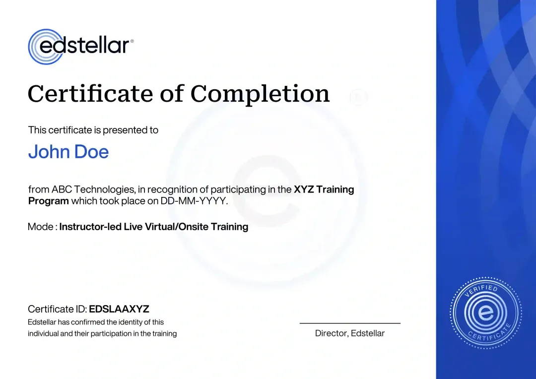
Certificate of Training Completion.
On successful completion, employees receive an Edstellar course completion certificate, recognizing their commitment to ongoing learning and professional development. It validates the skills they have built and motivates them to keep growing and contribute to organizational success.
Earned, not attended. Awarded on completion of all hands-on labs and the capstone project.
Training Delivery Modes: Virtual, Onsite and Hybrid
Choose the format that fits your design team: every mode includes live instruction and guided EDA labs with instructor coaching.
Hybrid Training
Blend live virtual sessions with onsite lab days, so distributed hardware teams learn together and practice on their own workstations.
- Live virtual instruction plus onsite lab days
- Same curriculum and labs in every batch
- Instructor coaching across both formats
- Flexible scheduling around project work

Onsite Training
The instructor delivers the full program at your facility, with labs run on your team's workstations and EDA licenses.
- Full program delivered at your office
- Labs on your team's own workstations
- Examples adapted to your board designs
- Direct review of your real schematics

Live Virtual Training
Join live from anywhere: instructor-led sessions with screen-shared EDA labs and one-on-one coaching for every participant.
- Live instructor-led virtual sessions
- Screen-shared guided EDA labs
- One-on-one coaching during lab time
- Recordings and lab guides included

Need a training format that works for your team?
Full days, half days across weeks, or split by module. Tell us the delivery window and we schedule the cohort around it.
Frequently Asked Questions
Share your team size, timelines, and delivery preference, and we will send a detailed per-group quote with batch options.
Yes. A short discovery call aligns the program with your boards, EDA tools, and team skill levels before scheduling.
Yes. Guided EDA labs run fully in live virtual sessions with instructor screen-sharing and one-on-one coaching.
Yes. Onsite delivery is available for teams that want instructor-led sessions at their own design workstations.
The program runs 24 instructor-led hours, typically scheduled across flexible batches that fit your team's calendar.
Question not answered here?
Put it in the request. A training specialist answers it directly, within one business day.
Where this Training Fits in Your Team's learning path.
Circuit design sits between hardware design basics and board layout. Your team learns hardware design, designs PCB circuits in this course, lays them out in Altium, and finally programs the board as an embedded system.

Why Choose Edstellar as Your PCB Circuit Design Corporate Training Provider
Edstellar delivers instructor-led PCB Circuit Design training with guided EDA labs, expert hardware practitioners, and a graded capstone, so your team ships fabrication-ready boards with fewer respins.

EXPERT TRAINERS
YEARS DELIVERING
ORGANIZATIONS TRAINED
CERTIFIED
Tailored
Examples, stackups, and the capstone board are adapted to your products, components, and fabrication partners.
Proven Methodology
A structured path from schematic capture to routed, reviewed boards, refined across real hardware design teams.
Practice-Based Learning
Every module pairs live instruction with guided EDA labs, so skills transfer to your next board project.
Expert Trainers
Sessions are led by electronics engineers who design and ship production boards, matched to your team's stack.
Global Scale
Train distributed hardware teams together in live virtual sessions, with consistent labs and review standards.
Measurable Outcomes
Lab reviews and a graded capstone measure design quality, so you see board readiness improve cohort by cohort.
Build PCB Designs With Traceable Libraries, Constraints, and Review Evidence
Edstellar develops PCB design discipline through a complete microcontroller-board project. Participants validate libraries, review schematics, and route a constrained multilayer layout before examining signal, power, and EMC considerations. The final handoff is assessed for consistency and documented checks, connecting electrical intent with the fabrication and assembly package.
- Step 01
Consult
We explore circuit and EDA familiarity to identify gaps in library quality, schematic review, placement and routing constraints, power delivery, and fabrication preparation.
- Step 02
Plan
We establish PCB and stackup foundations before libraries and schematic review, then develop constrained routing and integrity analysis ahead of the complete board package.
- Step 03
Align
We align electronics design and review expertise with hardware and embedded teams, calibrating support to their EDA tools, circuit foundations, and fabrication experience.
- Step 04
Customize
Sample microcontroller circuits, component libraries, and four-layer constraints reflect relevant product needs, enabling tailored layout reviews without treating one rule set as suitable for every board.
- Step 05
Execute
Participants verify symbols and footprints, clear schematic checks, route constrained layouts, and inspect power and signal behavior, receiving feedback on peer-review findings and manufacturing considerations.
- Step 06
Evaluate
We assess the board for consistent library and BOM data, resolved electrical and layout checks, documented integrity reasoning, and a coherent fabrication handoff with review evidence.
Also from Edstellar
Talent assessments
Psychometric, behavioral, leadership and 360-degree assessment.
→Training needs analysis
Needs analysis, gap identification, and a training roadmap.
→L&D consulting
Learning strategy, content, technology and ROI measurement.
→OD consulting
Org design, succession planning and cultural change.
→Managed training services
Training outsourcing, vendor management, logistics and administration.
→Coaching solutions
Executive and manager coaching that keeps skills in use.
Start an RFP shaped to your needs.
Answer three quick questions about team size, scope, and how often you need the program run, then send the request from the last step. Everything you choose travels with it, so you only fill this in once.
How many team members need training?
PCB Circuit Design Training Training Packages & Pricing
Where L&D holds an annual budget, license packages price the whole year at once instead of raising a purchase order per workshop. Hours and licenses are pooled across teams, programs and locations, so unused capacity is not stranded in one department.
Starter
120
trainee licenses64 hours of group training
Tailored for SMBs
Growth
320
trainee licenses160 hours of group training
Ideal for growing SMBs
Enterprise
800
trainee licenses400 hours of group training
Designed for large corporations
Custom
Unlimited
trainee licensesDuration set by the rollout
Multi-region and multi-year
Training Packages & Pricing
Choose the training format that works for your team. Pricing is customized based on your requirements, cohort size, and delivery needs.
Request PCB Circuit Design Training for Your Team
Share your team size, EDA tools, board complexity, and timelines to receive a tailored training plan and quote. Book a discovery call to discuss your goals; we confirm availability and respond with a proposal.