
PCB and Electronics Design with Altium Corporate Training
Give your engineering team the Altium Designer fluency to ship reliable boards, first pass.
Build the PCB design skills your team needs to move boards from concept to fabrication with confidence. Edstellar's PCB & Electronics Design with Altium corporate training program helps your electronics engineers master schematic capture, multilayer layout, high-speed routing, and design for manufacturing through instructor-led sessions with hands-on labs in Altium Designer. As the corporate training company enterprises trust for emerging-technology programs, we tailor every workshop to your board types, products, and goals.
Instructor-led group trainingVirtual / on-site / off-site10 languagesDelivered inEnglish, Spanish, Mandarin, German, Arabic, Portuguese, Hindi, French, Japanese, Italian100+ countriesWe have delivered inUnited States, United Kingdom, India, Canada, Germany, France, Netherlands, UAE, Saudi Arabia, Singapore, Australia, Japan, Brazil, South Africa and 90+ more countries
How we build board-ready engineering teams
THE EDSTELLAR PCB & ELECTRONICS DESIGN CAPABILITY MODEL
Baseline hardware fluency
Assess how your engineers rate schematics, layout, and the board decisions they already face.
Set one design standard
One shared language for schematic capture, layout, routing, and review across the hardware team.
Practice real board work
Guided design labs apply Altium Designer workflows to your board types, stackups, and constraints.
Prove the design lift
Before-and-after lab reviews measure each engineer's grasp of layout and signal integrity practice.
Scale across the business
One PCB design standard rolls out across teams and cohorts as your hardware portfolio grows.





Need more than one program?Get a group quote
Trusted as a Leading Corporate Training Provider by
















Program Overview: What is PCB and Electronics Design with Altium Corporate Training?
PCB & Electronics Design with Altium is a 24-hour program for electronics engineers, hardware designers, and embedded teams learning professional board design. It covers electronics foundations, Altium workspace setup, schematic design, and component libraries. Participants learn stackup design, placement, routing, signal and power integrity, and design for manufacturing.
Training is lab-driven, with each module anchored in Altium Designer exercises led by PCB design practitioners. Participants capture schematics, build libraries, lay out boards, and tune routing for signal and power integrity. Instructors review layouts directly, coaching on stackup choices and manufacturing readiness. The capstone takes a board from concept to fabrication outputs, including Gerbers.
Bad layouts cause respins that cost weeks and thousands of dollars in fabrication and assembly. This program teaches designers to get stackup, placement, and routing right the first time and design for manufacturing from the start. Boards stop failing in fab and start working on the bench.
The capstone board is the proof: each participant designs a complete PCB in Altium, from schematic capture through layout to fabrication-ready outputs, defended against instructor review. That board file becomes a portfolio artifact they can show any employer, demonstrating professional-grade design skills rather than tutorial knowledge.
Across six modules, your engineering team moves from electronics foundations to a capstone board delivered as a fabrication package. Sessions use real-world use cases, your board constraints, and Altium Designer labs, so every technique transfers directly to your products.
Delivered as a hybrid instructor-led program, it fits around your calendar, with scheduling set along with you, and content tailored to your board types and industry.
What's Included in this Workshop for Your Enterprise Teams
- 1
Altium workspace foundations
Workspace setup, project structure, and design rules.
- 2
Schematic and library work
Clean schematics and managed component libraries.
- 3
Layout and placement
Stackup planning and manufacturable placement.
- 4
Routing and integrity
High-speed routing, signal and power integrity.
- 5
DFM and fabrication outputs
DFM checks, Gerbers, BOMs, and assembly data.
- 6
Capstone board project
A complete board from concept to fabrication package.
- Training delivered at any of your offices globally
- 10+ languages
- Schedule around your calendar
- Group size set along with you
- Run as one cohort or split into batches
- Instructor-led (virtual/onsite/hybrid)
- Recurring and annual options
- Trainer sourcing, matching and logistics
Build your team's skills. Anywhere in the world.
Real-world use cases
from day one
Instructor-led training
for your teams
Delivered globally
in 100+ countries


Enterprise Training Solutions Customized for Your Company
One partner for instructor-led corporate training, delivered the way your teams work.
Request a Training Quote- Customized Training Delivery
- Scale Your Training: Small to Large Teams
- In-person Onsite, Live Virtual or Hybrid Training Modes
- Plan from 2000+ Industry-ready Training Programs
- Hands-On Labs on Live Infrastructure, Led by Industry Experts
PCB and Electronics Design with Altium Course Topics and Program Outline
A tailored 28-hour, seven-module workshop: one learning journey from 6G ISAC foundations and sensing theory to a capstone prototype. Sessions pair concepts with guided labs on waveform design, sensing pipelines, and mmWave simulations. Materials include simulation templates, joint-performance report frameworks, and security hardening checklists, plus a capstone design review.
Built by Edstellar with PCB design and electronics engineering practitioners
Built by engineers who design and manufacture printed circuit boards with Altium in production, shaped around your stack and use cases.
Baseline each participant's PCB design readiness before module 01 begins
Build strong PCB design foundations in instructor-led sessions for your team
Reinforce skills through guided hands-on labs in Altium Designer board workflows
Apply PCB design skills to real-world scenarios and a capstone board design project
A short pre-training assessment sets each participant's entry level, so the program starts where your team actually is. The rest is weighted toward hands-on practice: guided Altium labs, design reviews, and realistic board scenarios drawn from your team's work, not slides.
Delivered as
Entry level set by the assessment. Depth and schedule customized to your team.

Set up your Altium workspace, configure design rules, and test your baseline electronics fluency on a sample board.
learna)Reading datasheets and circuit fundamentals refresher
b)Altium Designer workspace, panels, and preferences
c)Project structure, schematic documents, and version control
d)Setting up design rules and project options
e)Navigating the unified design environment end to end
Build schematic symbols and footprints for a real component set, then capture a clean hierarchical schematic.
practicea)Drawing clean, reviewable schematics in Altium
b)Building schematic symbols and footprint libraries
c)Library management and component lifecycle
d)Net classes, ports, and hierarchical design
e)Schematic review checklist and annotation
Plan a 4-layer stackup and place components for a mixed-signal board, ready for manufacturability review.
practicea)PCB stackup planning for 2, 4, and 6 layer boards
b)Component placement for manufacturability and test
c)Design rules for clearances, annular rings, and masks
d)Grounding strategies: planes, pours, and splits
e)Placement lab: positioning a real mixed-signal board
Route differential pairs and a power distribution network, then run power integrity checks with the PDN Analyzer.
practicea)Interactive routing techniques and length tuning
b)Differential pairs and controlled impedance routing
c)Power distribution networks and decoupling strategy
d)High-speed design rules: crosstalk, return paths, vias
e)Power integrity simulation with Altium PDN Analyzer
Run DFM checks against a fabrication partner rule set and generate a complete fabrication and assembly package.
applya)Design for manufacturing, assembly, and test rules
b)Generating Gerber, drill, and ODB++ fabrication outputs
c)Assembly drawings, pick and place files, and BOMs
d)Running DFM checks and closing review feedback
Design, route, and release a complete board in the capstone project, then present it for expert review.
applya)Capstone brief: requirements to board specification
b)Full schematic, layout, and routing of the capstone board
c)DFM sign-off and fabrication package generation
d)Design review presentation and bring-up plan
Customize this program tailored to your team?
Tell us your training needs: what your team already works with, the level they’re at, and the topics you want them to focus on. We’ll adjust the modules, duration and hands-on labs, and send you a customized outline for your group.
Key Skills and Outcomes Your Team Will Gain
Your engineers will leave able to design, route, and release multilayer boards in Altium Designer. Each outcome is practiced in hands-on labs and shown in the capstone board project.
Set up Altium Designer projects
Configure the workspace, panels, design rules, and project options for a professional board design workflow.
Draw production-ready schematics
Create clean hierarchical schematics with custom symbols and managed component libraries.
Lay out multilayer PCBs
Plan stackups and place components for manufacturability, testability, and reliable assembly.
Route high-speed and power circuits
Route differential pairs and power networks with signal and power integrity discipline.
Apply design-for-manufacturing rules
Pass DFM, assembly, and test checks before a board ever leaves for fabrication.
Generate fabrication and assembly outputs
Produce Gerbers, drill files, ODB++, BOMs, and pick-and-place data for your manufacturing partners.
Deliver a board from concept to fabrication
Take a real design through review and release in the capstone project.
Teams that Benefit from this PCB and Electronics Design with Altium Group Training
This program is built for engineering teams designing electronics products, from hardware engineers to firmware and manufacturing teams. No prior Altium experience is needed; content adapts to each cohort's board types and products, so every engineer practices the design decisions their role actually owns.
Design boards your products can rely on.
Hardware engineers master schematic capture, multilayer layout, and signal integrity in Altium Designer, so boards pass review and fabrication the first time.
Workflow friction
- Board respins burn schedule and budget
- Signal integrity issues found too late
- Inconsistent design practices across the team
How the program helps
- Cut respins with disciplined layout and DFM
- Route high-speed interfaces with confidence
- Apply one Altium design standard
Practice use cases
- Schematic capture
- Multilayer layout
- High-speed routing
Bring up the boards you designed.
Embedded engineers learn board-level design fundamentals and test-point planning, so bring-up and debugging go faster on the boards they own.
Workflow friction
- Bring-up stalls on boards they did not design
- No visibility into board design decisions
- Hardware-software integration surprises
How the program helps
- Read and review board designs fluently
- Plan test points and debug access up front
- Shorten bring-up and integration cycles
Practice use cases
- Board bring-up
- Design reviews
- Test planning
Take boards from design to production.
Product and manufacturing engineers learn DFM rules, BOM management, and fabrication outputs, so designs move cleanly from engineering to your manufacturing partners.
Workflow friction
- Fabrication rejects and DFM rework
- BOM and assembly data errors
- Cost surprises from board complexity
How the program helps
- Pass DFM checks before fabrication
- Produce clean BOMs and assembly data
- Control board cost through smarter design
Practice use cases
- DFM sign-off
- BOM management
- Supplier handoffs
Each cohort works through role-relevant design labs, then leaves with a capstone board and a shared Altium design standard.
Prerequisites: No prior Altium Designer experience is needed. What helps most is basic electronics knowledge, such as voltage, current, and reading a simple circuit, plus day-to-day work on electronic products or boards. We cover workspace setup and licensing guidance in the first module, and content adapts to each cohort's board types, so hardware, embedded, and manufacturing engineers learn side by side.
Electronics Engineer to Hardware Design Leader
The program takes engineers from Altium fundamentals to production-grade board design: foundation schematic and layout skills, intermediate high-speed routing and integrity work, then advanced DFM and a capstone board release.
Engineers grow from board fundamentals to owning complete Altium design delivery as the modules progress.
Mixed cohort, or several teams at once?
We can tailor the training to different teams, roles, and experience levels within the same program.
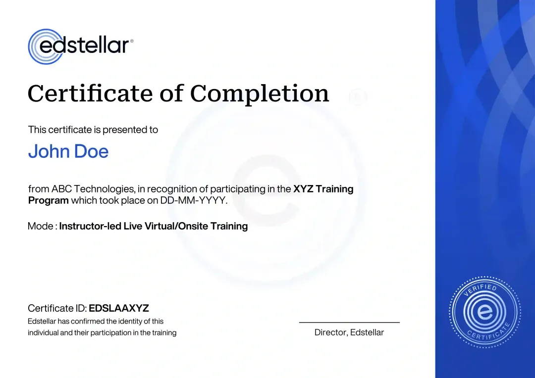
Certificate of Training Completion.
On successful completion, employees receive an Edstellar course completion certificate, recognizing their commitment to ongoing learning and professional development. It validates the skills they have built and motivates them to keep growing and contribute to organizational success.
Earned, not attended. Awarded on completion of all hands-on labs and the capstone project.
Training Delivery Modes: Virtual, Onsite and Hybrid
Every mode is shaped around your board types before delivery. The curriculum, hands-on labs, and capstone stay the same in each format, so what your engineers can do after training never depends on how you run it.
Hybrid Training
Live instruction across office and remote sessions, with hands-on Altium labs coached throughout. Your engineers capture schematics, route boards, and run DFM checks with instructor guidance. Best for multi-site teams.
- Live instruction across office and remote sessions
- Hands-on Altium labs with instructor coaching
- Real-world board designs and DFM scenarios
- Best for engineers across sites and time zones

Onsite Training
Your instructor delivers at your facility, with labs set up for your engineering team. Participants design, route, and review boards with direct coaching. Best for co-located teams.
- Instructor delivers at your facility
- Labs set up for your team and board types
- Direct coaching during design work
- Best for co-located teams wanting maximum interaction

Live Virtual Training
Live virtual sessions on Zoom or Microsoft Teams, with remote Altium labs and screen-shared guidance through every task. Your engineers collaborate on board designs in real time. Best for distributed engineering teams.
- Live sessions on Zoom or Microsoft Teams
- Remote access to the Altium lab environment
- Screen-shared guidance through every task
- Best for distributed engineering teams

Need a training format that works for your team?
Full days, half days across weeks, or split by module. Tell us the delivery window and we schedule the cohort around it.
Frequently Asked Questions
Share your team size, preferred dates, and delivery mode in the lead form. We reply with a tailored proposal covering scope, schedule, and pricing for your group.
Both. Choose live virtual sessions on Zoom or Teams, onsite delivery at your office, or a hybrid mix across sites and time zones.
The standard program runs 24 hours of instructor-led sessions, typically over three to four days. We can reshape the schedule around your calendar.
We recommend 10 to 16 engineers per cohort for strong lab coaching. Larger teams can run as parallel batches.
No. The program starts with workspace setup and assumes no prior Altium experience; basic electronics knowledge is all that helps.
Question not answered here?
Put it in the request. A training specialist answers it directly, within one business day.
Where this Training Fits in Your Team's learning path.
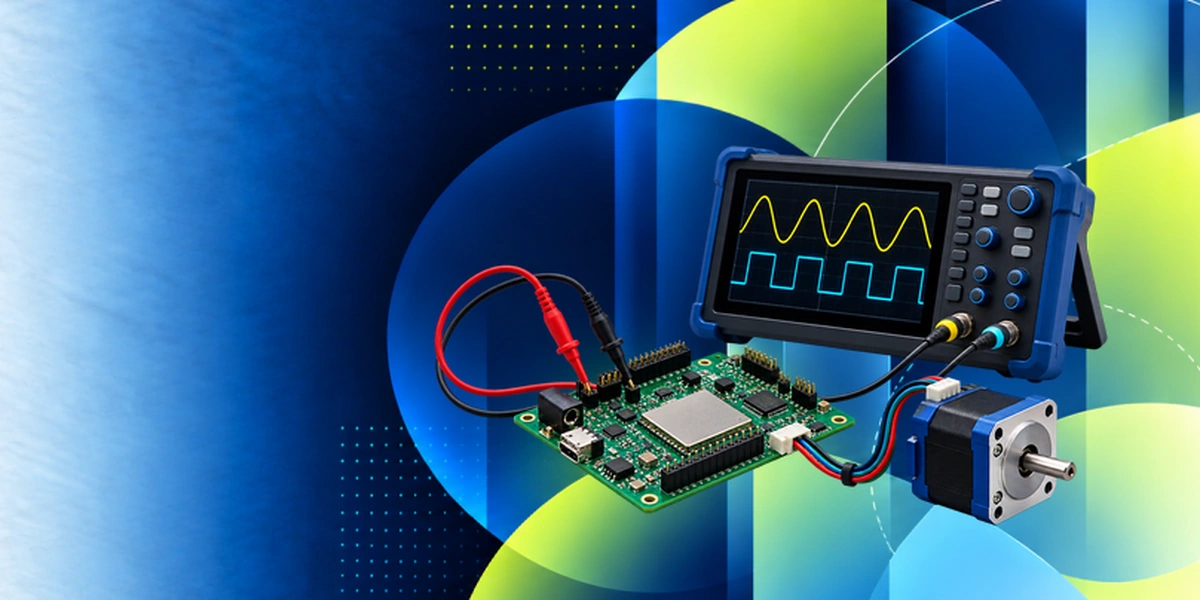
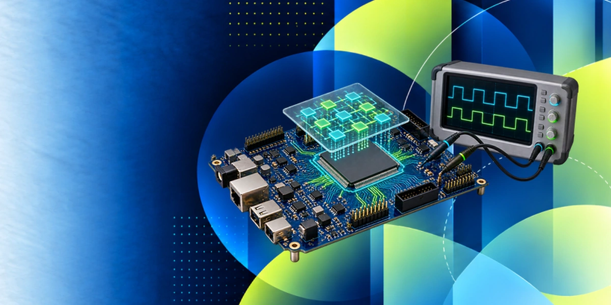
Altium layout comes after circuit design: your team designs the circuit, then lays out the board in Altium in this course. The path continues with programming the finished board as an embedded system, and ends with FPGA design for more demanding hardware.
Why Choose Edstellar as Your PCB and Electronics Design with Altium Enterprise Training Provider
If your engineering team needs to ship reliable boards on schedule, start here. Tell us about your board types, timelines, and preferred delivery mode, and we will shape a program around them.
EXPERT TRAINERS
YEARS DELIVERING
ORGANIZATIONS TRAINED
CERTIFIED
Tailored
Content shaped around your PCB design and electronics engineering in Altium use cases, mapped to your team's real work.
Proven Methodology
5+ years delivering corporate training to hardware and embedded engineers across industries and regions.
Practice-Based Learning
6 hands-on labs across 6 modules. Your team builds fabrication-ready PCB designs with instructor guidance.
Expert Trainers
5,000+ certified trainers matched to your PCB design with Altium, with a full trainer profile shared before your program is booked.
Global Scale
One PCB design training program across your offices worldwide, in hybrid, onsite, or live virtual.
Measurable Outcomes
Baseline-to-capstone measurement and Skills Matrix reporting keep your PCB and electronics design capability lift visible.
Develop Altium Boards With Coherent Schematics and Verified Fabrication Outputs
Edstellar connects electronics design decisions across the Altium workflow. Participants build libraries and schematics, plan a multilayer board, and examine routing and power behavior before preparing manufacturing outputs. The final board package is reviewed for consistent constraints, documented checks, and a clear handoff from circuit intent to fabrication and assembly information.
- Step 01
Consult
We assess electronics knowledge and board responsibilities to identify gaps in Altium setup, library accuracy, schematic structure, constrained layout, and manufacturing handoff.
- Step 02
Plan
We establish workspace and design rules before schematics and components, then develop stackup, routing, and integrity checks ahead of fabrication outputs and board review.
- Step 03
Align
We align PCB and Altium expertise with hardware, embedded, and manufacturing roles, confirming suitable workspace and tool arrangements while adapting support to participants' electronics foundations.
- Step 04
Customize
Sample mixed-signal circuits and component sets reflect relevant board types, enabling tailored stackup and routing exercises while preserving explicit manufacturing constraints and review criteria.
- Step 05
Execute
Participants build hierarchical schematics, route differential pairs, and examine PDN Analyzer results, receiving feedback on Altium rule checks and manufacturing outputs.
- Step 06
Evaluate
We review the Altium board project, power-integrity checks, and fabrication package for consistent constraints, explained routing decisions, and complete assembly information.
Also from Edstellar
Talent assessments
Psychometric, behavioral, leadership and 360-degree assessment.
→Training needs analysis
Needs analysis, gap identification, and a training roadmap.
→L&D consulting
Learning strategy, content, technology and ROI measurement.
→OD consulting
Org design, succession planning and cultural change.
→Managed training services
Training outsourcing, vendor management, logistics and administration.
→Coaching solutions
Executive and manager coaching that keeps skills in use.
Start an RFP shaped to your needs.
Answer three quick questions about team size, scope, and how often you need the program run, then send the request from the last step. Everything you choose travels with it, so you only fill this in once.
How many team members need training?
PCB & Electronics Design with Altium Training Packages & Pricing
Where L&D holds an annual budget, license packages price the whole year at once instead of raising a purchase order per workshop. Hours and licenses are pooled across teams, programs and locations, so unused capacity is not stranded in one department.
Starter
120
trainee licenses64 hours of group training
Tailored for SMBs
Growth
320
trainee licenses160 hours of group training
Ideal for growing SMBs
Enterprise
800
trainee licenses400 hours of group training
Designed for large corporations
Custom
Unlimited
trainee licensesDuration set by the rollout
Multi-region and multi-year
Training Packages & Pricing
Choose the training format that works for your team. Pricing is customized based on your requirements, cohort size, and delivery needs.
Request PCB and Electronics Design with Altium Training for Your Team
Share your team size, board types, preferred delivery mode, and timelines. We will respond with a tailored training plan covering scope, schedule, and pricing, and confirm trainer availability.